Why Is Semiconductor Precision Machining So Demanding?
Semiconductor precision machining covers parts that operate inside wafer fabs and chip assembly lines—wafer-handling fixtures, probe cards, lead frame dies, and the tooling that shapes them. Tolerances land in the micron range, and the materials resist normal cutting. Knowing why the bar sits so high matters. It tells you which specs actually drive performance and which are just noise on a drawing.
Demanding here is not marketing. The strictness traces back to process risk. A positioning feature that locates a wafer affects every layer aligned on it. A probe tip that lands off-pad fails a test. Each part’s requirement level depends on its role in that chain, not on a blanket industry rule. The sections below cover where the strictness comes from, how it translates into materials, tolerances, and surfaces, and what to verify before you pick a supplier.
Where the Strictness of Semiconductor Precision Machining Comes From
The pressure does not start at the machine shop. It starts at the device and travels down through the equipment that makes it. In semiconductor precision machining, the chain starts at the wafer. This section shows how requirements distribute across parts by their function in the error chain, and why the cost of a miss justifies hard minimums.
Why Do Semiconductor Parts Need Tight Tolerances?
Device features are nanometer-scale. That alone does not force every carrier, bracket, or fixture to the same size tolerance. What matters is where the part sits in the chain. A wafer locating feature positions every exposure on that wafer. A probe pattern decides whether test needles contact the right pads. These parts carry functional requirements. Support brackets do not.
The useful framing for why semiconductor parts need tight tolerances is not “the industry is strict.” These specific features directly influence device results. Position error in a locator becomes overlay error in lithography. The magnification happens step by step, from fixture to stage to exposure. Yield loss from positioning errors is a core concept in semiconductor manufacturing.
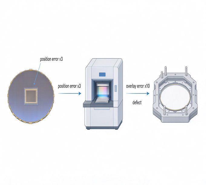
What Does a Failed Part Cost on a Production Line?
Precision here is about yield — the share of usable chips per wafer. One mislocated wafer can misalign an entire layer. One drifting probe pattern can take out an entire test station. A defective component can cause localized quality issues, disrupt a test process, or contribute to production downtime, depending on its function and where the failure occurs. This potential impact is why critical tooling and fixture requirements must be tied to specific performance risks and verified through inspection.
Fabs run around the clock, and wafers carry many high-value dies. That is why requirements are written as hard minimums, not “as tight as practical.” The cost of a miss is not rework. It is lost production.
What Demanding Semiconductor Precision Machining Requires
Strictness lands in three checkable places: material behavior, tolerance definition, and surface condition. This section turns “high precision” into engineering requirements you can verify. It closes with a short checklist for evaluating a shop.
Which Materials Make Semiconductor Machining So Hard?
Most semiconductor tooling is not aluminum. It is tungsten carbide, hardened tool steel, ceramics, and engineering plastics. Each limits machining and verification differently.
Machining tungsten carbide for semiconductor fixtures is hard mainly because of its hardness and wear resistance. Carbide blunts ordinary cutters quickly. The right process depends on grade and geometry — grinding for round features, EDM for shapes a wheel cannot reach.
Hardened steel (typically 55–62 HRC) often needs grinding or wire EDM. But the choice depends on part shape, stock removal, heat-treatment state, and surface integrity requirements—not hardness alone.
Ceramics add brittleness and thermal sensitivity. The difficulty varies with ceramic type, processing stage, and target surface quality. PEEK and similar plastics raise different issues: dimensional stability under heat, tool sharpness, and avoiding smeared surfaces. Each material requires different processes and a verification method.
How Tight Is Tight for a Semiconductor Fixture?
No single number applies to all fixtures. Tolerance is set per feature, by function. A locating-pin position, a bore roundness, a contact-face flatness, and a repeatability spec are different indicators. Mixing them up is where over-specification starts.
Semiconductor machining tolerance microns describe the working scale, not a universal value. Ask what each critical feature needs: position relative to which datum, flatness over which area, roundness at which bore. The drawing should name the feature, the value, and the measurement method.
Why Does Surface Finish Matter for Semiconductor Tooling?
Surface requirements follow function. A contact face that seals or mates may need a low Ra and no burn layer. A non-contact surface does not. Surface finish requirements for semiconductor tooling therefore vary by feature, not by a single standard applied to every face.
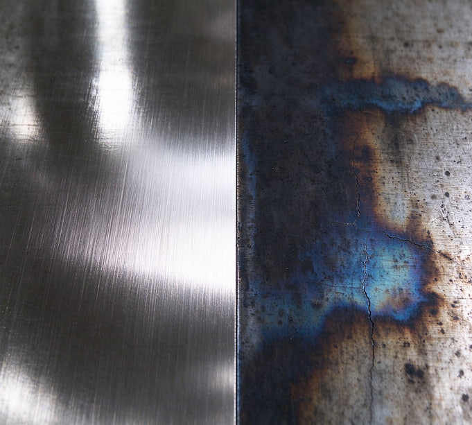
Underneath roughness sits surface integrity. Grinding carbide or hardened steel too hot can leave a burned or re-cast layer. It can look fine and fail early. For critical surfaces, the specification may need to address more than Ra. Depending on the application, it may also define acceptable surface integrity, limits on grinding burn or EDM-related damage, and requirements for dimensional stability. Select these requirements based on the component’s function and verify them using suitable inspection methods.
Which Parts Need This Level of Control?
Not every semiconductor part is micron-critical. The parts that need tighter control are those whose dimensions, positioning, or surface condition directly affect product handling, testing, tooling performance, or equipment accuracy.
- Wafer handling fixture machining — carriers, chucks, and end-effectors that grip wafers. Repeatability, flatness, and particle-free surfaces matter more than absolute size.
- Semiconductor probe fixture precision — probe cards and test fixtures where hole patterns must match device pads.
- Lead frame die machining — stamping tools that run at high speed, where every stroke must land the same.
Support brackets, covers, and frames that never touch product can use standard CNC tolerances and finishes. Over-specifying those wastes budget without buying reliability.
What Should You Confirm Before Specifying Semiconductor Tooling?
Start by looking for what to expect in a semiconductor machine shop before comparing suppliers. Confirm four things:
- Does the part touch the wafer, chip, or forming tooling? That decides whether micron-level work applies.
- Are tolerances tied to named features and measurement methods — or just optimistic numbers on a drawing?
- Does the shop’s process list match the material and geometry? Carbide and 60 HRC steel need specific processes.
- Is surface integrity specified, or only roughness? Ask how they control burning, smearing, and residual stress.
Where sub-micron machining for semiconductor work applies, capability shows up in habits: temperature-controlled grinding, calibrated EDM, and same-day measurement. A closer look at precision tooling manufacturing capabilities is worth it. The machine list and process specs tell the story better than any summary.
Semiconductor precision machining is demanding for a reason: process risk. Requirements cascade down from the device, and each part carries only as much precision as its role demands. Materials limit process choice. Tolerances and surfaces must be tied to named features. The strictness was never arbitrary — it is how a line full of nanometer-scale devices stays profitable.