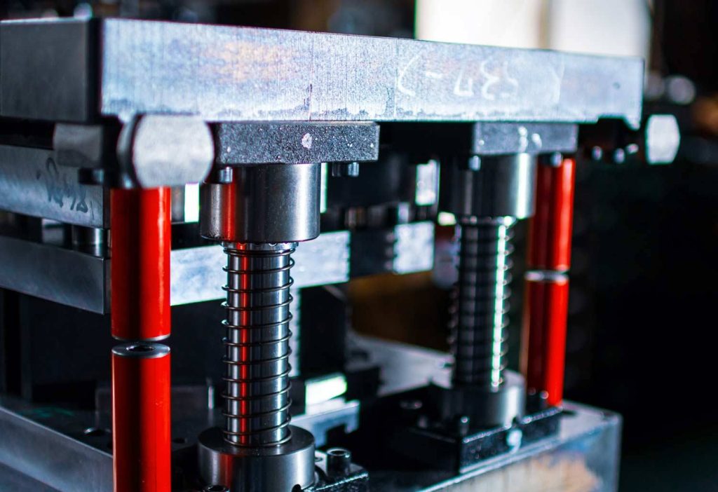
The Role of Precision Die and Stamping in Consumer Electronics Miniaturization?
Miniaturization is a core trend in today’s consumer electronics. As smartphones, wearables, and IoT devices shrink in size, their internal components must also shrink in size. Precision Die and Stamping offers manufacturers the accuracy and consistency required to meet these new size constraints. Unlike traditional methods, this process shapes and cuts ultra-small parts with exact tolerances, ensuring a perfect fit within tight spaces. Supporting Lightweight and High-Density Assemblies To maintain portability, consumer electronics must remain lightweight and compact. Precision stamping enables the use of thinner materials without losing strength or functionality. It also supports complex geometries that would be challenging with machining. As a result, designers can pack more features into less space. Additionally, Precision Die and Stamping contribute to high-density component layouts. With accurate tool control, parts can be made to tight specifications repeatedly. This allows for multi-layered assemblies, which are crucial in smartphones and tablets, where every millimetre counts. Stamped components also offer excellent consistency, minimizing rework and defects. Enabling Integration of Advanced Features Modern devices often incorporate cameras, sensors, wireless modules, and additional components. These features require exact placement and mechanical reliability. Precision Die and Stamping delivers parts that support this integration. They can produce frames, connectors, and EMI shields with the required micro-level tolerances. Additionally, as device functions increase, thermal and mechanical loads rise. Stamped metal parts can be engineered for heat dissipation or structural reinforcement. This ensures that even the smallest devices remain stable and safe to use. Integration becomes feasible only when each micro-component performs as intended. Maintaining Efficiency at Scale Consumer electronics are produced in massive volumes. Any manufacturing method must scale efficiently. Precision Die and Stamping is inherently scalable due to its repeatability and tooling life. Once a die is created, it can yield millions of identical components with minimal variation. This not only supports consistency but also reduces per-unit cost over time. Moreover, since tooling changes are infrequent, downtime is reduced. For companies looking to maintain margins in competitive markets, stamping offers both high precision and economic viability. The process aligns perfectly with the needs of large-scale production. Meeting Industry Standards and Certification Requirements The electronics industry is tightly regulated. Every part must meet stringent quality, safety, and environmental standards. Precision Die and Stamping technologies are well-suited to meet these expectations. By maintaining tight tolerances and surface finishes, they ensure compliance with global benchmarks. From RoHS to IPC specifications, stamped parts often undergo automated inspection. This enhances traceability and quality control. Additionally, the process is compatible with cleanroom manufacturing, which is crucial for producing parts used in sensitive environments, such as medical devices or advanced computing systems. Enabling Sustainability Through Material Efficiency Sustainability is a growing concern. Manufacturers must reduce waste while maintaining performance. Precision Die and Stamping enable near-net-shape production, minimizing excess material. Scrap rates are lower than those in traditional subtractive processes, such as machining. Furthermore, the process supports the use of recyclable metals. This aligns with environmental goals and helps reduce the carbon footprint of electronics manufacturing. Combined with high repeatability and efficiency, stamping is an eco-conscious choice that offers no performance trade-offs. Adapting to Emerging Consumer Electronics Trends The rise of foldables, wearables, and augmented reality demands even greater precision. These new formats involve moving parts and flexible displays. Precision Die and Stamping can create hinges, conductive paths, and support structures to enable these designs. Because stamping supports intricate features and miniaturization, it’s key to adapting to future devices. As form factors become more diverse, the flexibility of the stamping process ensures it can meet varied and evolving design requirements. Its role continues to expand as devices evolve. Precision die and Stamping are Foundational Technologies for Miniaturization Precision Die and Stamping are foundational technologies in the ongoing miniaturization of consumer electronics. They enable smaller, lighter, and more powerful devices without compromising quality or production scale. Their precision ensures seamless integration of advanced features and compliance with rigorous standards.
